What Is Layout Design Rules In Vlsi

Layout Rules

Electronic Systems 2015 Cmos Design Rules Youtube

Cmos Design Rule
Layout Design Rules 2 Introduction Layout Rules Is Also Referred As Design Rules It Is Considered As A Prescription For Preparing Photomasks Ppt Download

Design Rule Checking Wikipedia

Lambda Based Design Rule Hindi Youtube

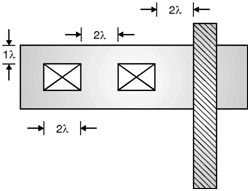
Design or layout rules.
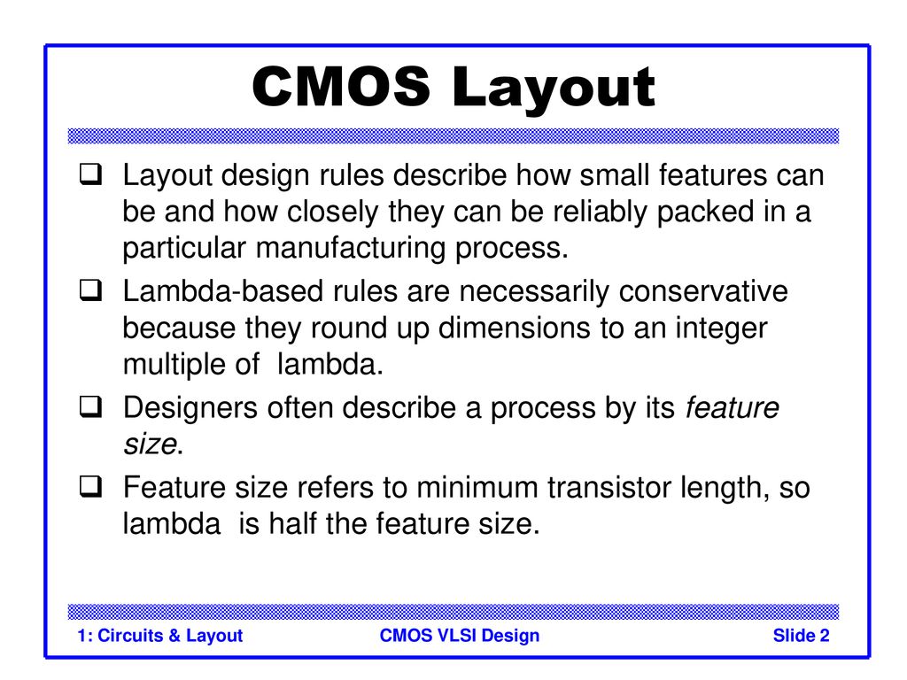
What is layout design rules in vlsi. Main terms in design rules are feature size width separation and overlap. Design rules ensure that design is still functional even when there may be lots of misalignments and various side effects of the fabrication process. 2 design rules cmos vlsi design slide 3 layout overview minimum dimensions of mask features determine. In the cad or say eda electronic design automation world to verify these rules different tools are developed by the eda vendors commonly known as drc design rule checking or checks tools.
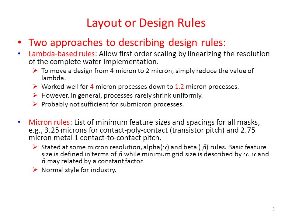
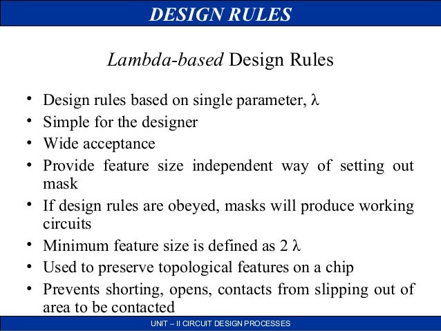
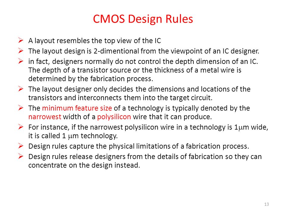
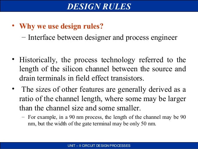
Transistor size and die size hence speed cost and power historical feature size f gate length in nm set by minimum width of polysilicon other minimum feature sizes tend to be 30 to 50 bigger. The most important parameter used in design rules is the minimum. Design rules does represent geometric limitations for for an engineer to create correct topology and geometry of the design. Layout design rules.
Design Rules
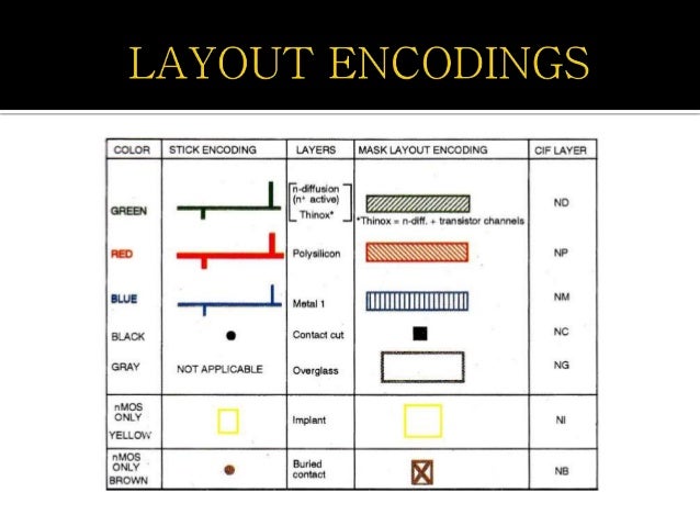
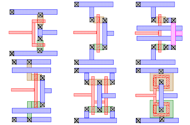
Layout Stick Diagram Design Rules

Layout Design Rule Cmos Field Effect Transistor
Design Of Vlsi Systems Chapter 3

Layout Design Rules Design Rule Check Drc Vlsi Concepts
Vlsi Circuit Design Process

Cmos Design Rules And Packaging Electronic Systems 2017 Youtube
Layout Design Rules 2 Introduction Layout Rules Is Also Referred As Design Rules It Is Considered As A Prescription For Preparing Photomasks Ppt Download

Design Of Vlsi Systems Chapter 3
Vlsi Circuit Design Process

Introduction To Layout Design Rules
Layout Design Rules
Cmos Lambda Design Rules Digital Cmos Design Electronics Tutorial