What Is Layout Design In Vlsi

Cadence Tutorial
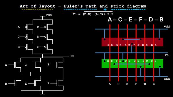
Art Of Layout Euler S Path And Stick Diagram Part 3 Vlsi System Design
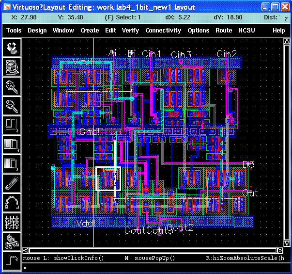
Ece 658 Vlsi Design Lab 4 A
Integrated Circuit Layout Wikipedia
Layout Stick Diagram Design Rules
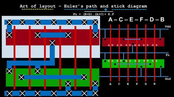
Art Of Layout Euler S Path And Stick Diagram Part 3 Vlsi System Design
Vlsi layout design wednesday august 13 2008.
What is layout design in vlsi. The microprocessor is a vlsi device. 69 describe six different layout strategies that are commonly used to minimize the possibility of latch up. The compression of the layout from all directions to minimize the chip area thereby reducing wire lengths. Very large scale integration vlsi is the process of creating an integrated circuit ic by combining thousands of transistors into a single chip.
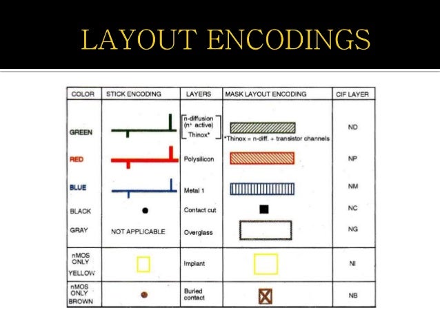
9 cmos vlsi design standard cell layout layout slide 17 layout cmos vlsi design slide 18 gate layout standard cell design methodology vdd and gnd should be some standard height parallel within cell all pmos in top half and all nmos in bottom half preferred practice. Design rules does represent geometric limitations for for an engineer to create correct topology and geometry of the design. Vlsi began in the 1970s when complex semiconductor and communication technologies were being developed. Layout design rules are introduced in order to create reliable and functional circuits on a small area.
Subsystem design and layout of vlsi section 6 1. Before the introduction of vlsi technology most ics had a limited set of functions they could perform. This is particularly so in the case of the design of avlsi system which could otherwise take so long as to render the whole system obsolete before it is off the drawing board. Main terms in design rules are feature size width separation and overlap.
Why is it a serious concern in cmos layout design. The smaller the chip size can get the better it is. 70 why is it wise to plan designs to make it easier to change details later. The physical design is the process of transforming a circuit description into the physical layout which describes the position of cells and routes for the interconnections between them.
The main concern is the physical design of vlsi chips is to find a layout with minimal area further the total wire length has to be minimized.
Design Vlsi Layout And Schematic On Cadence By Ex Einstien Pal

Cmos Layout Design Introduction Vlsi Concepts
Ic Layout

How To Draw A Layout In Magic Vlsi Youtube

Vlsi What Are Standard Cell Layout Analog Custom Layout Quora

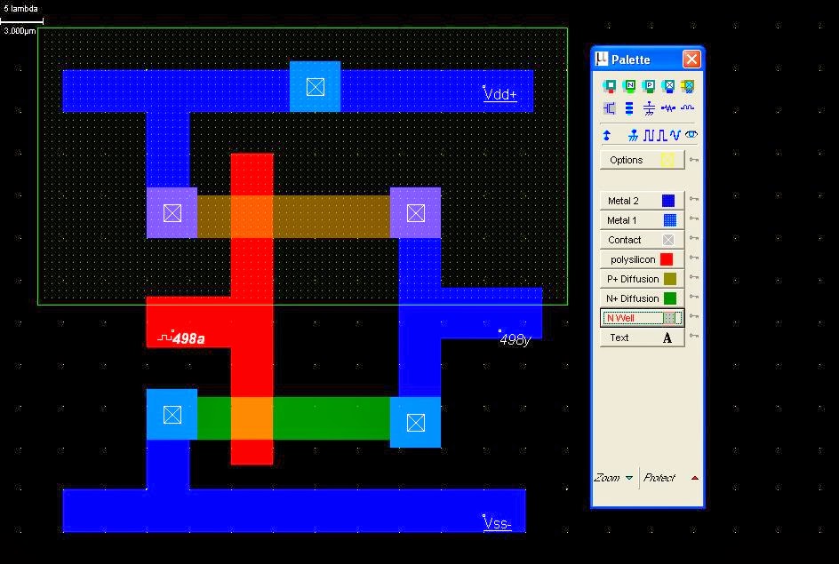
Layout Rules

Magic Vlsi Layout Tutorial Part 1 Youtube
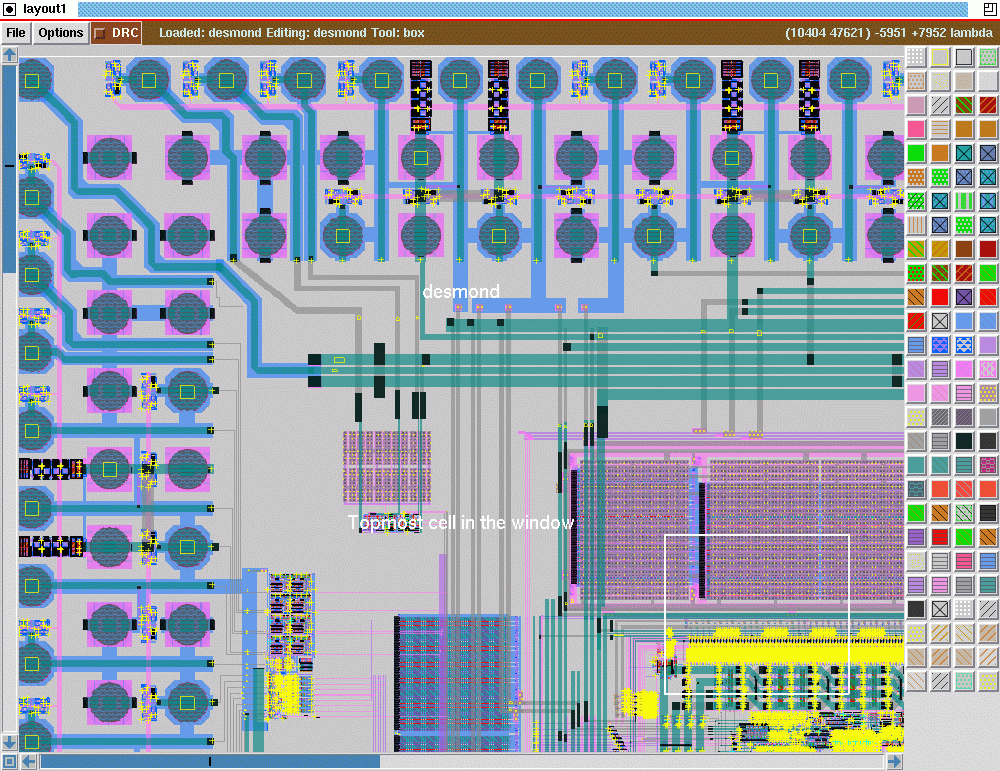
Magic Vlsi
Design Rules
Crazy Ece Rocks Vlsi Layout Designs
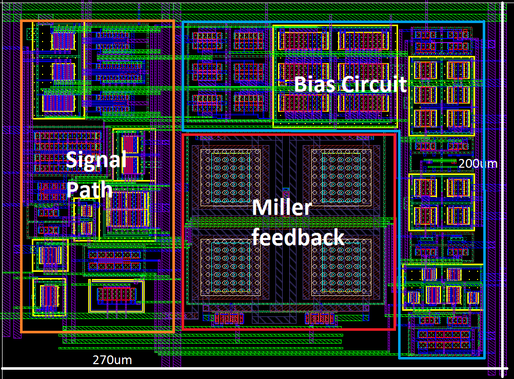
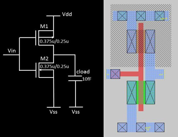
Physical Layout Design Example Download Scientific Diagram
Let S Do Some Magic Vlsi System Design

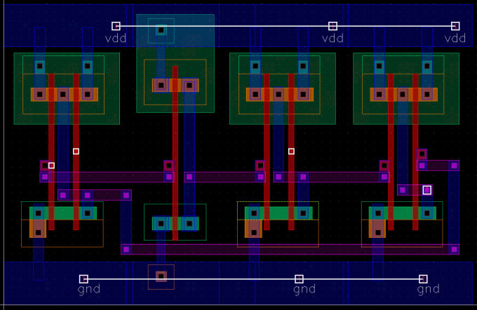
Layout Design Of Pll With Four Output Download Scientific Diagram